


MYIR SoM Leverages Zynq UltraScale+ with Arm and FPGA Integration
Jan 3, 2026 — by Giorgio Mendoza 358 views MYIR has announced the MYC-CZU3EG-V3, an updated SoM built around the AMD Zynq UltraScale+ ZU3EG MPSoC. The module integrates application-class Arm processing, real-time control cores, and FPGA fabric in a compact form factor targeting industrial automation, machine vision, edge computing, aerospace, and telecommunications systems.
The MYC-CZU3EG-V3 combines a quad-core Arm Cortex-A53 application processor running at up to 1.2 GHz with a dual-core Cortex-R5F real-time subsystem clocked at up to 600 MHz. Hardware acceleration and deterministic I/O are handled by programmable logic fabricated on a 16 nm FinFET process, while graphics output is supported by an Arm Mali-400 MP2 GPU.
— ADVERTISEMENT —
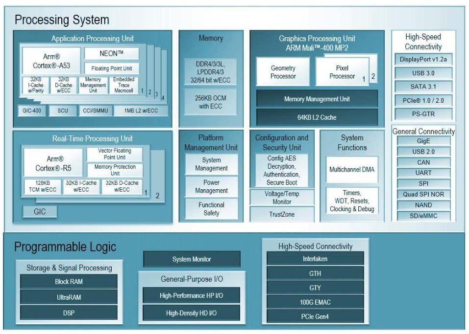
AMD Zynq UltraScale+ EG Processor Block Diagram
Memory on the module consists of 4 GB of DDR4 SDRAM, paired with 8 GB of onboard eMMC and 64 MB of QSPI flash. MYIR integrates key system components directly on the SoM, including Gigabit Ethernet and USB PHYs, power management, and clock generation, allowing the module to operate as a minimal standalone embedded system.
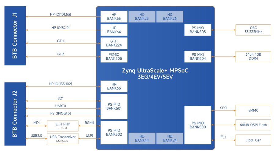
MYC-CZU3EG-V3 SoM Functional Block Diagram
High-speed connectivity is exposed through two 160-pin, 0.5 mm-pitch board-to-board connectors. These provide access to interfaces such as PCIe Gen2 x4, USB 3.0, SATA 3.1, DisplayPort 1.2a, SD/SDIO, and multiple serial buses including UART, CAN, SPI, and I2C, alongside a wide range of FPGA I/O.
The ZU3EG programmable logic exposes substantial FPGA resources, including DSP blocks, block RAM, and multiple AXI interfaces for hardware acceleration and deterministic data paths.
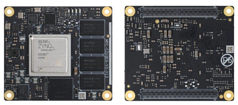
MYC-CZU3EG-V3 SoM
For evaluation and prototyping, MYIR offers the MYD-CZU3EG-V3 development board, which mounts the 60 x 52 mm SoM and breaks out its interfaces to standard connectors.
The carrier board provides USB 3.0, Gigabit Ethernet, DisplayPort, PCIe, SATA, HDMI, CAN, SD card support, JTAG, Arduino-compatible headers, PMOD, FMC, and optional display interfaces.
It ships with an active heatsink preinstalled on the SoM and is positioned as both an evaluation platform and a reference design for custom carrier development.
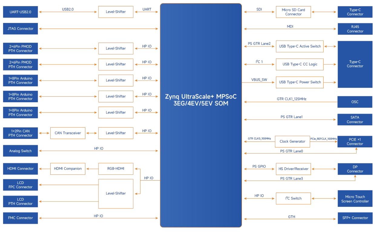
MYD-CZU3EG-V3 Dev Board Functional Block Diagram
Software support includes a ready-to-run Linux 6.6.40 platform based on PetaLinux 2024.2, with U-Boot 2024.01 and a customized kernel.
MYIR supplies a full SDK and board support drivers for major interfaces such as PCIe, SATA, USB, Ethernet, CAN, DisplayPort, HDMI, and SD, along with prebuilt HDMI and LCD PetaLinux images and corresponding source code. The platform also supports AMD Vitis for heterogeneous Arm-FPGA software development.
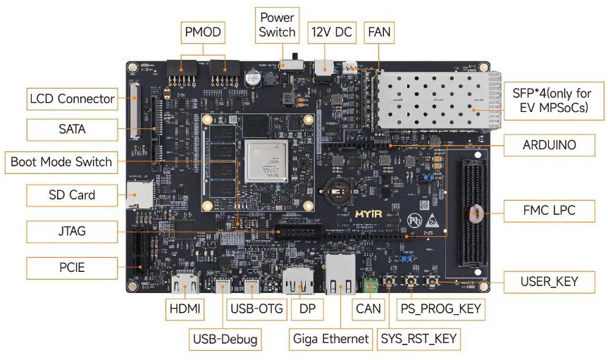
MYD-CZU3EG-V3 Development Board
MYIR also notes support for Yocto Project-based Linux distributions, with Linux kernel 6.12 listed among the supported releases. Android support is mentioned by the vendor, with details available on request.
Specifications listed for the MYC-CZU3EG-V3 SoM include:
- Processor / FPGA:
- AMD Zynq UltraScale+ XCZU3EG MPSoC
- 154K system logic cells
- 141K CLB flip-flops
- 71K CLB LUTs
- 360 DSP slices
- 7.6 Mb block RAM
- 1.8 Mb distributed RAM
- 12 × 32/64/128-bit AXI PS-to-PL interfaces
- Quad-core Arm Cortex-A53 (up to 1.2 GHz)
- Dual-core Arm Cortex-R5F real-time processors (up to 600 MHz)
- Arm Mali-400 MP2 GPU (up to 667 MHz)
- AMD Zynq UltraScale+ XCZU3EG MPSoC
- Memory:
- 4 GB DDR4 SDRAM (64-bit, 2400 MHz)
- Storage:
- 8 GB onboard eMMC
- 64 MB QSPI flash
- Display:
- DisplayPort 1.2a
- Connectivity:
- Gigabit Ethernet (onboard PHY)
- PCIe Gen2 x4
- SATA 3.1
- USB 3.0
- SGMII Ethernet
- I/O Interfaces:
- GPIO, 2× CAN 2.0B
- 2× UART, 2× SPI, 2× I²C
- SD / SDIO
- USB:
- 1× USB 3.0
- 1× USB 2.0
- Power:
- 3.3 V input
- Integrated power management
- Clock generator
- Watchdog timer
- Operating Temperature:
- 0 °C to +70 °C (Commercial grade)
- −40 °C to +85 °C (Industrial grade)
- Mechanical:
- 60.0 × 52.0 mm
- 14-layer PCB
- 2x 160-pin Samtec B2B connectors
Further Information
Samples of the MYC-CZU3EG-V3 SoM and the MYD-CZU3EG-V3 development board are available now. MYIR lists pricing starting at $319 for the commercial-grade SoM and $339 for the industrial-grade version.
The MYD-CZU3EG-V3 development board is priced at $429 for the commercial model and $449 for the industrial variant, with volume discounts available. More details can be found on MYIR product pages.

Please comment here...